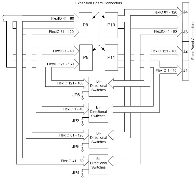
The following diagram shows the connectors associated with the expansion board (P8 to P11) and the bi-directional switches used to connect the Flex I/O signals directly to the front panel connectors depending whether jumpers J3 to J6 are installed or not.
An option the user has when designing his application is the ability to select in groups of 40 I/O channels which signals will go to the daughter board and which signals will go directly to the front panel connectors.
By selectively connecting JP3, JP4, JP5, and JP6 the user can route I/O channels to the front panel connectors or the daughter card in groups of 40 I/O channels depending on the needs of the application.

GX3500 Expansion Board Connectors and Bi-Directional Switches Block Diagram
The bi-directional switches, when enabled by connecting their respective jumpers, will be turned on and the corresponding signals between the Flex IO and the front panel connectors will be permanently connected, these are pass-through switches and there is no direction control signal. When developing a design, the user needs to be aware that signals that are either inputs or outputs only are defined as inputs or outputs on the FPGA, these signals can be left driving or enabled all the time; however signals that are bi-directional like bus signals need to be defined as bi-directional on the FPGA but make sure to drive the output to high impedance or tri-tristate level when the signal is not driving or is inactive. This will prevent signal contention if two signals connected to the same switch from opposite directions are turned on or enabled at the same time.
Programming expansion board is done using the GXFPGA registers and memory access functions. In addition a GxFpgaSetExpansionBoardBypass can be used to direct the I/O banks to the expansion board. The GxFpgaGetExpansionBoardID can also be used to detect the installed expansion board ID. The expansion board ID is read from P8 pins 19, 21, 23 and 25 to form a 4-bit integer (0-15).