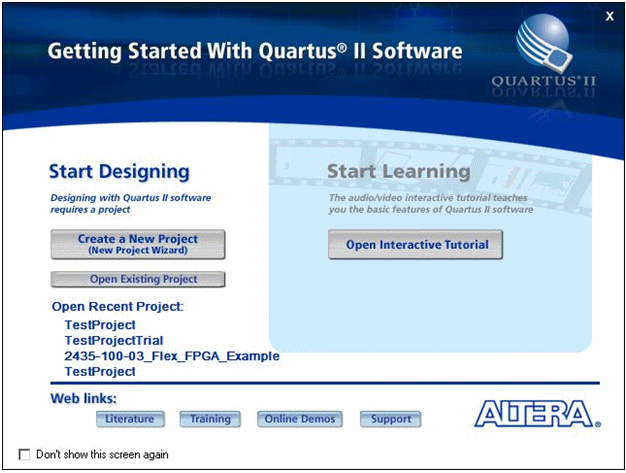

Quartus II Start Dialog
After installing Quartus II Web Edition, start the application and select Create a new Project to start the New Project Wizard or select File, New, New Quartus Project.
Click on Next and then select the Project Folder and enter FPGATutorial as the project name.
Click on Next twice (skip the adding files window).
The next window will allow you to select the FPGA target device. Select Cyclone III as the Family and EP3C55F484C8 as the Available Devices selection.
Click on Next twice (skip the Specify Tools window).
A window summarizing all the choices made for the creation of this project is shown. Click on Finish.
You should now have an empty skeleton project loaded in Quartus II. Before you can get started on the FPGA design, you must assign the FPGA pins distinct names so that you can reference them in your design. This can be accomplished by running a TCL script which contains all the information necessary to configure the pin assignments. These pin assignments are unique to this the Cyclone III FPGA and the GX3500 in particular. The following table lists all the pin assignments and their respective descriptions. The Pin Alias’s listed in the table are the pin names you will be using in your design to reference the actual hardware pins on the FPGA.
Pin Alias (Node Name) |
Description |
Clocks |
|
10Mhz |
10 MHz Reference Clock Signal from the PXI Backplane. |
PCIClock |
33 MHz PCI Bus clock. |
RefClk |
80 Mhz Reference Clock onboard the GX3500. |
RefClka |
80 Mhz Reference Clock onboard the GX3500. |
PCI Bus |
|
Addr[2..19] |
The PCI Address lines from the PCI bus. |
FDt[0..31] |
PCI Data lines from the PCI bus. |
CS[1..2] |
CS[1] is for PCI BAR1 and CS[2] is for PCI BAR2. |
RdEn |
PCI Read Enable line from the PCI bus. |
WrEn |
PCI Write Enable line from the PCI bus. |
PXI Bus |
|
PxiTrig[0..7] |
PXI Bus trigger signals. |
StarTrig |
PXI Star Trigger signal. |
I/O |
|
FlexIO[1..160] |
The physical IO Channels. |
Misc |
|
Spare[0..2] |
Do Not Use. |
IRQ |
Interrupt input pin, Pulse width >20nSecRising edge (transition from 0 to 1) activates the IRQ, falling edge (transition from 1 to 0) clears the IRQ. |
Spare[4..6] |
Do Not Use. |
FSpr[0..5] |
Spare Signals from the User FPGA and Expansion Board. |
MClr |
FPGA Master Clear, Active Low. |
TP[0..5] |
Test Points located on the GX3500 PCB. |
To configure the pin assignment first the .TCL configuration script should be added to the project. To add the script to the project, right click on the Files icon in the Project Navigator window and click on Add/Remove Files in Project… In the dialog box, click on the … button and browse for GX3500Pins.tcl file in the C:\Program Files\Marvin Test Solutions\GXFPGA folder. Click Open and then the Add button.
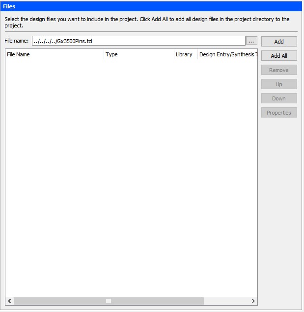
Add Tcl Script to Project
Then click on Tools | TCL Scripts … Select the configuration script file, GX3500Pins.tcl and click on Run. This will configure your FPGA pin assignments.
Later versions of the Quartus toolset may not execute the script through the GUI. Instead, the script can be executed in the Tcl console using the following command:
source <filename>
Where <filename> is the path to a TCL script. For example:
source C:\Program Files (x86)\Marvin Test Solutions\GxFpga\Gx3500Pins.tcl
You can view the pin assignments by running the Pin Planner application which is found in the Tasks list as highlighted below:
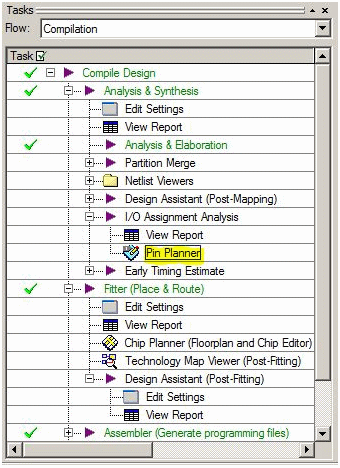
Task Flow
The Pin Planner will display a matrix of the physical FPGA pins and their mapped names as well as the I/O standard supported by the pin. These mapped names are used in the FPGA design, as wire names and I/O pins, to connect to the physical connections of the FPGA.
You must now create a design file as part of the project. Click on File, New, Block Diagram/Schematic File as shown in the figure below. Go to File | Save As and name the file TutorialDesign and click OK. The new design file, TutorialDesign.bdf will be added to your project. Right click on the file and select Set As Top-Level Entity. Double click on it to open the file. You will be presented with a blank schematic view.
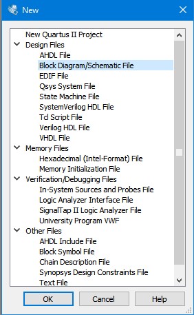
New Block Diagram
You can now begin schematic entry.
Note: There is more than one way to accomplish the following designs.