Now that the design has been completed, compiled and loaded into the Gx3500, we can move on to the testing.
There are two ways to access the FPGA, either through the software front panel or through the driver API DLL. We will demonstrate the programming method using ATEasy to access the driver API DLL.
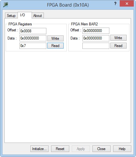
The software front panel will be used to test Phase 1 of the design which adds two 32 bit numbers together. Click on the I/O Tab to get started. The Adder phase is controlled through the FPGA Register space.
Offset 0x0 points to the first 32-bit number that will be summed and offset 0x4 points to the second 32-bit number that will be summed. Write values to both these locations.
The sum can be obtained by reading the 32-bit value at offset 0x8. Verify that the correct sum is read back as shown in the figure below.

Using the Software Front Panel to read back the Sum
The software front panel will once again be used to test Phase 2 of the design. This part of the design uses a Mux to select between the PCI Clock and the 10 MHz reference clock. The selected clock is output to I/O Channel 33 which is located on pin 31 on the Flex I/O A connector of the GX3500. The Mux is controlled through the FPGA Register space.
Writing a 0x0 to offset 0xC will route the 33 MHz PCI Clock signal to I/O Channel 33. Writing 0x1 to the same offset will route the 10 Mhz clock to I/O Channel 32. Try switching between both values while monitoring pin 31 with an oscilloscope. You should see the appropriate clock signals.
For this test, connect an oscilloscope to I/O Channel 1 (pin 35) to monitor the output signal of the sequencer. You can access the FPGA memory through the software front panel or through ATEasy. When using the software front panel, write values to the first 32 double words of the FPGA Memory space (offsets 0x0, 0x4, 0x8, 0xC etc.). As you write to these locations, the data patterns being output on I/O Channel 1 should be updating dynamically. If you fill the 32 double word memory with a clock pattern (alternating 1’s and 0’s), you should be able to measure a frequency of 100KHz.
When using ATEasy, include the GxFPGA.drv driver and set it up with the correct slot number. Add a variable called i of type long. You can then run the following code to write to the FPGA memory:
REDIM adwData[32]
adwData[0] = 1
For i=0 to 31
FPGA Write Memory(i*4, 4, adwData[i])
Next
This code will set the first double word to 1 and the rest to 0‘s resulting in a frequency of 6.25 Khz.