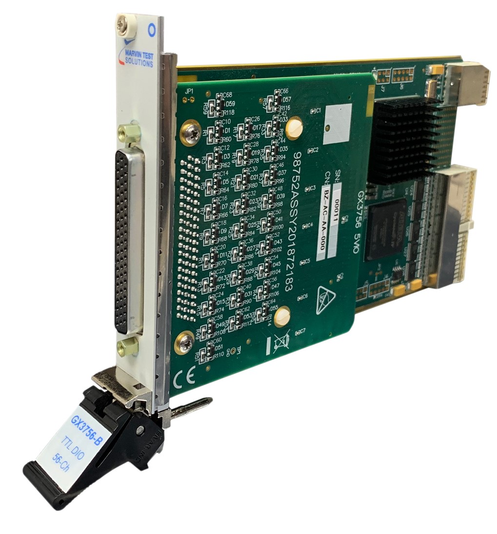
The GX3756 Discrete I/O module is consists of a standard GX37xx carrier card, a unique daughter board and a dedicated firmware loaded into an FPGA. The GX3756 has 56 5V TTL I/O channels and 3 input channels. Every four channels have a common output enable line. Four channels can be used for custom serial data communication. The daughter card of GX3756 has output buffers and protection circuits.
The GX3756 has fourteen I/O groups of four channels each. There are registers that allow the user to set the output level of each channel, enable the outputs of each group and read the level of each I/O pin. The user can also read the status of the connector ID lines, open or short to ground.
Group 0 of the GX3756 I/O can be selected to operate as serial data transmitters. Once one channel is selected for serial data all the group outputs are enabled.
The transmission is 30 bits. Each bit period is 1mS. When transmitting ‘1’, the line goes high for 640uS and then low for the rest of the period. When transmitting ‘0’, the line goes high for 320uS and then low for the rest of the period. The user can set the 30 bits and a trigger source. Once triggered, the 30 bits will be transmitted.
Use the Gx3756xxx driver functions to program the board. The functions are described in detail in GX3756 Functions section. Some of the functions are also available from the software front panel.

GX3756 Board