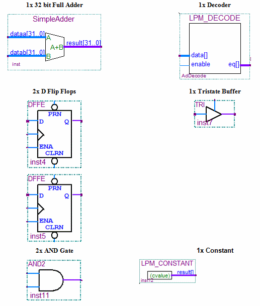
This design will take two double word (32 bit) values, located in the first two double words in the Register space (byte offset 0x0 and 0x4), and add them together. The sum of the two values will be immediately output to the third double word in the Register space (byte offset 0x8).

Phase 1 Adder Components
In order to open the schematic view, click on File menu, and then New the following dialog appears.
Select Block Diagram/Schematic File:
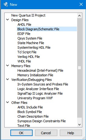
Open Schematic view Dialog Box
First start with creating the circuitry required to decode the PCI Address when data is to be written from the PC to the FPGA. This circuit will be used in all three functions of this example project. The signals required for PCI Write access will be the PCI Clock, Write Enable, Chip Select 1, and some PCI Address lines. The PCI Address lines 5 to 2 will be fed to a decoder which will generate a 32-bit value, and the result will be ANDed with the Chip Select 1 bit. Each Chip Select bit represents a certain PCI BAR access (GX3500 has two bars, memory and register memories). Bit 1 represents BAR1 of the PCI memory space (bit 2 for BAR2). BAR1 is the general-purpose Control Register BAR for the GX3500. The results of the AND operation will be once again ANDed to the Write Enable PCI signal.
Double click on the blank space in the schematic view and select lpm_decode from the Megafunction, Gates directory.
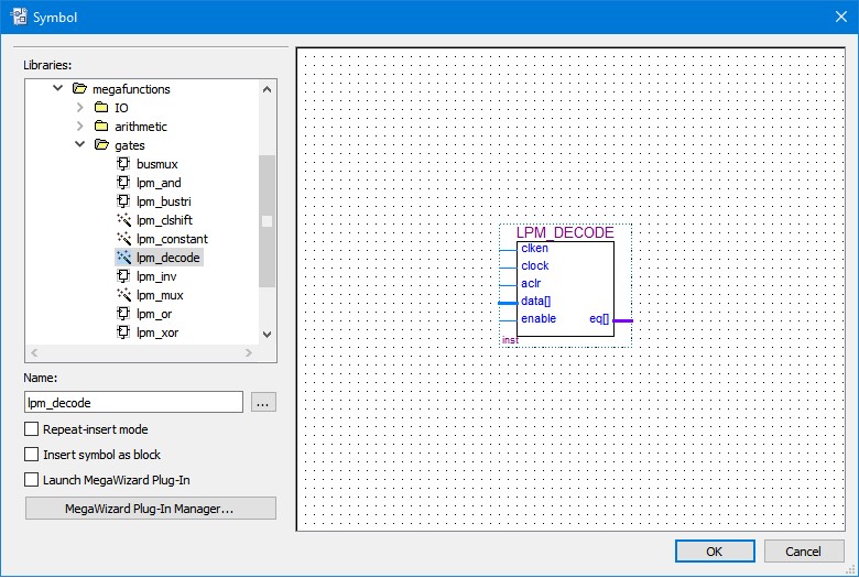
Symbol Insert Dialog Box
Make sure the Launch MegaWizard Plug-In checkbox is unchecked.
Click OK and place the symbol on the blank design document.
Now that the Decoder has been placed, some of its parameters have to be set. Right click on the Decoder symbol and select Properties. Click on the Parameters tab. Set the Width and Decodes properties as shown below:
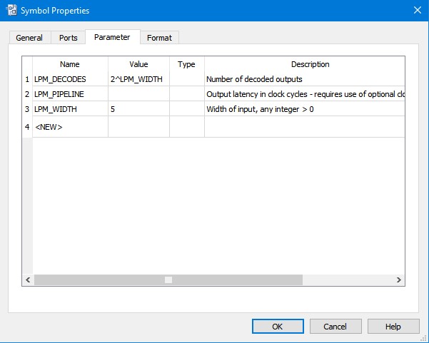
Decoder Properties
Click OK when done. Place another symbol on the design by double clicking on the design document, and selecting Input Pin from Primitives, Pin, Input. After placing the input pin symbol, rename it to Addr[6..2]. The symbol will now represent 5 PCI address lines that will be used to communicate with the PC.
Also place 2 AND gates after the Decoder and a few more input pins with the appropriate names DecAddr, Sel and WE as the following figure shows:

PCI Address Decoder Circuit
Note: To wire several signals together (as a bus), such as Addr[6..2] or Sel[31..0], use the Bus Wiring Tool highlighted in red below. We use two D-Flip-Flops to clean up the signal going into our design before we use it.

Bus Wiring Tool
Now that the PCI address decoder circuit is complete, we can feed the appropriate bits from the WE bus to D Flip Flops that will store data clocked in from the PCI data lines. For example, the first double word in PCI memory (representing the first number to be summed) will be written to a D Flip Flop with it enables line tied to WE[0] (the first bit in the WE bus). The second double word to be added will be written to another D Flip Flop with it enables line tied to WE[1]. Finally, the PCI Clock signal (33Mhz) will be used as the clock source of the D Flip Flops. Note that each bit of the Sel and WE busses represent a consecutive double word address (bit 0 corresponds with byte 0, bit 1 corresponds with byte 4, bit 2 corresponds with byte 8 etc.)
Place two D Flips Flops (located at primitives, storage, dffe) and an input pin named PCIClock. We will leave the D Flip Flops input lines (D) disconnected for now. Eventually the PCI data lines will drive these inputs.
Wire the output of the AND gate to D Flips Flops as shown below.
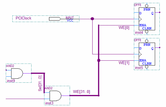
D Flip Flops
The D Flips Flops will feed a 32-bit adder and the resulting summation will be wired to the PCI data lines so that the PC can read the result.
The 32-bit adder will be placed onto the design using the MegaFunction wizard tool. This tool will customize a component by allowing you to make selections through a wizard.
Double click on the design window and navigate to megafunctions, arithmetic, lpm_add_sub. Make sure the Launch Megafunctions Wizard checkbox is selected and click OK. You will see a dialog box like the following:
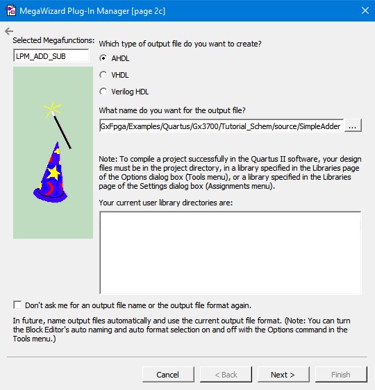
Adder Wizard
Name the output file SimpleAdder and make sure the path is the same as your project. Click Next and enter 32 as the data width.
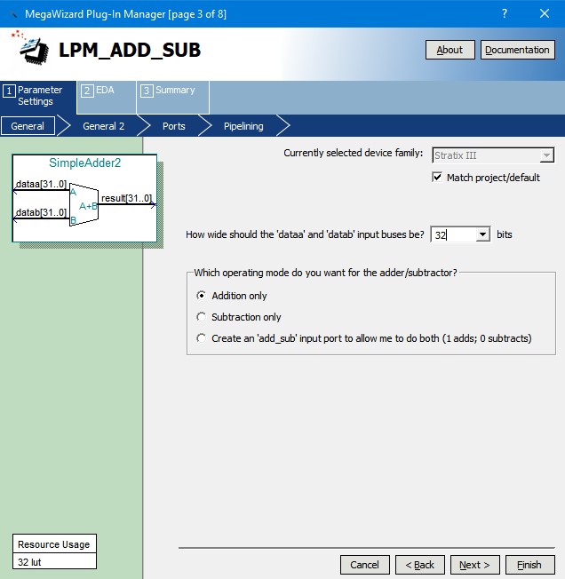
Adder Wizard 2
Click Next through the rest of the wizard and keep the default choices. Finally, the dialog box will show the newly created design files that will be included in your project. Click Finish and place the newly created Adder in your design.
Wire the adder to the flip flops and add an AND gate, Read Enable pin, and tristate buffer as the following shows:
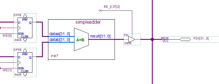
Adder Circuit
Note that we are using the FDt[31..0] PCI data lines as bidirectional pins since we will be reading and writing to the PCI bus. The Tristate buffer is used to select whether the Adder will be driving the PCI Data lines or not. The Tristate buffer is controlled by the 3rd bit of the decoded PCI Address ANDed with the Read Enable line. When both signals are high (Sel[2] and RdEn) it indicates that the PCI Bus is expecting the 3rd double word to be written to the PCI bus. In our case, this means the 32-bit result from the Adder.
Before moving on we must first extend the RdEn to 2 PCI clock cycles by adding a small circuit as demonstrated below:
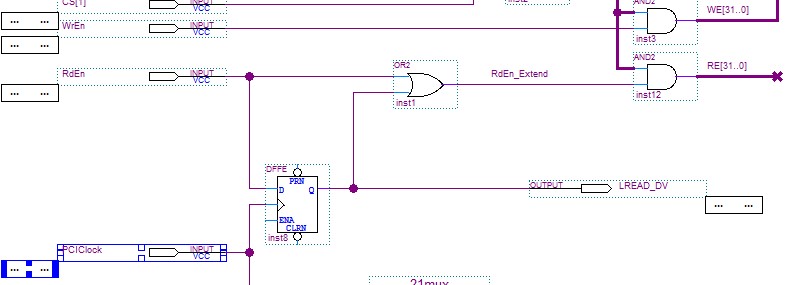
RdEn to 2 PCI Circuit
We also create a Read Data Valid output pin, LREAD_DV. This comes from a D-Flipflop with the PCIClock as an input clock and the RdEn as the input data. The D-Flipflop also creates our extender for our ReadEnable.
Since this design is created to be able to be implemented in both the 3700 and the 3700e, we need to extend our read enable pins, RE[31..0], for 3 more clock cycles. Below is the circuit to do that.
![RE[31..0] and WE[31..0] extend Circuit](RE_31..0__and_WE_31..0__extend_Circuit.jpg)
RE[31..0] and WE[31..0] extend Circuit
The inputs to the D Flips Flops can now be wired to the PCI data lines (FDt). We need to clean up the FDt signal as is comes back into our circuit by adding the D-FlipFlop.
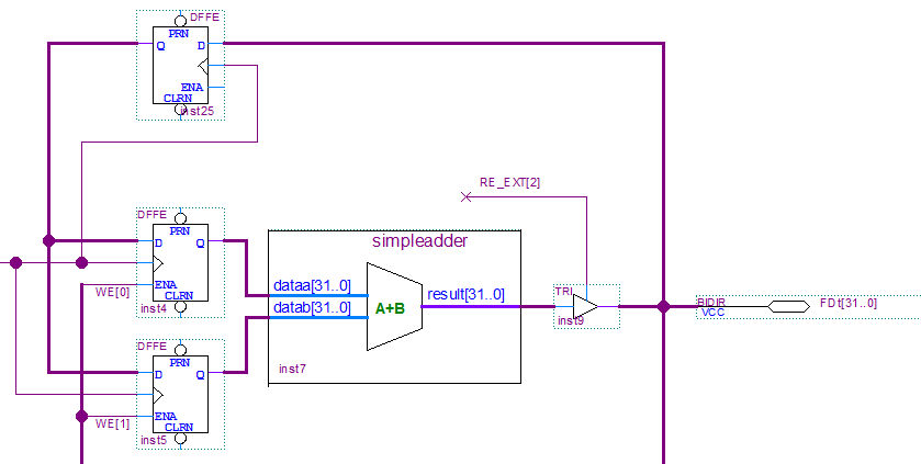
Adder Circuit with PCI Bus Connection
Now that the design has been completed, a revision number should be added so that the end user can read it back from the PCI bus at the 32nd register double word location (byte address 0x7C).
Including a revision number constant to the design is a Geotest standard practice that we recommend end users to follow. The revision constant is 32 bits long and is read as a hexadecimal number such as 0x3564A000. The first two digits of the hexadecimal number represent the company, in this case 35 is for Geotest designs. The next two digits are the design specific code, 64 in this case. And the last 4 digits, A000, is the revision of the design.
A constant component needs to be placed in the design (LPM_CONSTANT). When placing this component make sure that the “Launch MegaWizard Plug-In” selection is unchecked. After placing the component, right click on it and select properties to set the value and width of the constant as the following figures show:
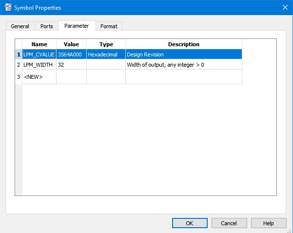
Symbol Properties
Now place the 2 port AND gate and the tri-state buffer. You can rotate it, as shown in the figure above, by right clicking on the symbol (after placing it) and select “Rotate By Degrees | 90”.
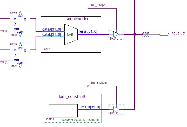
Adder Circuit with Revision Constant
Finally, you can change the inputs to the adder from write-only to read/write by connecting the output of the D-Flipflops to the FDt inout pin via a tristate buffer. After adding this buffer, the complete adder circuit should appear as below:
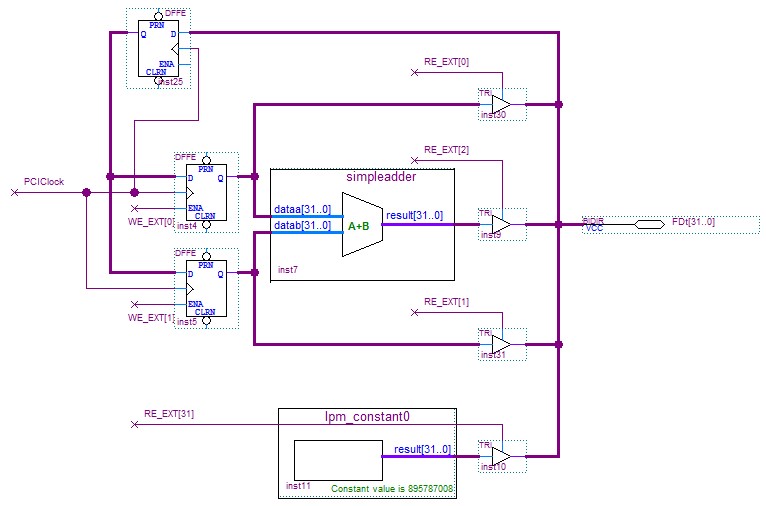
Completed Adder Circuit