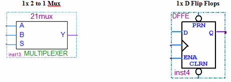
This design will output either the PCI Clock (33Mhz) or the 10Mhz clock to Flex I/O Channel 65 (check the connector tables to find the pin number) depending on what was written to the 4th double word in the PCI register space (byte offset 0xC). A 1 will select the 10Mhz clock signal, and a 0 will select the PCI clock signal.

Phase 2 Mux Components
You will now build upon the tutorial project to add the functionality of a 2 to 1 Clock Mux. The 10Mhz clock will be brought into the design by an input pin. The PCI Clock signal input pin is already present in the Phase 1 circuit, so this will be reused. FlexIO[65] (IO Channel 65) will be used to output the selected clock to the outside world.
Place the 2 to 1 Mux symbol by double clicking on the design area and selecting megafuncitons others, maxplus2, mux21.
Create three wires attached to the D, ENA(enable) and B inputs of the D Flip Flop. Name the wires FDt[0], Sel[3], and PCIClock respectively. Note that you did not have to place new input pins to access these signals. This is due to the fact that input pins were already created for these signals in the Phase 1 design. Therefore, you can just use named wires to tap into the same input pins.

Clock Mux Circuit
FDt[0] is the first bit of the PCI data bus. This bit can either be 0 or 1, to indicate which clock source to choose. Sel[3] is the 4th bit from the decoded PCI Address. When this bit is high, it indicates that the PCI Bus is addressing the 4th double word (byte offset 0xC) of the Register space for the GX3500. In our case, the value of this double word is used to select which clock is selected by our Mux.