
Quartus II Start Dialog
After installing Quartus II Web Edition, start the application and select Create a new Project to start the New Project Wizard or select File, New, New Quartus Project.
Click on Next and then select the Project Folder and enter tutorial_design_top as the project name.
Click on Next twice (skip the adding files window).
The next window will allow you to select the FPGA target device. Select Stratix III as the Family and EP3SL50F780C3 when using the GX3700 or EP3SL70F780C3 for the GX3700e. For newer GXFPGA boards, the device ID will be displayed in the instrument front panel About page.
Click on Next twice (skip the Specify Tools window).
A window summarizing all the choices made for the creation of this project is shown. Click on Finish.
You should now have an empty skeleton project loaded in Quartus II. Before you can get started on the FPGA design, you must assign the FPGA pins distinct names so that you can reference them in your design. This can be accomplished by running a TCL script which contains all the information necessary to configure the pin assignments as well as settings the project to either schematic entry or Verilog entry. These pin assignments are unique to this Stratix III FPGA and the GX3700 in particular. The following table lists all the pin assignments and their respective descriptions. The Pin Alias’s listed in the table are the pin names you will be using in your design to reference the actual hardware pins on the FPGA.
Pin Alias (Node Name) |
Description |
Clocks |
|
10Mhz |
Input. 10 MHz Reference Clock Signal from the PXI Backplane. |
PCIClock |
Input. 33 MHz PCI Bus clock or 125MHz PCI Express application clock. |
RefClk |
Input. 80 Mhz Reference Clock onboard the GX3700. |
PCI Bus |
|
Addr[2..19] |
Input. The PCI Address lines from the PCI bus. |
FDt[0..31] |
Bidir. PCI Data lines from the PCI bus. |
CS[1..3] |
Input. Chip
Select lines from the PCI bus. |
LEXT |
Input. External SRAM chip select. This is chip select for external SRAM on PCB. |
RdEn |
Input. PCI Read Enable line from the PCI bus. |
WrEn |
Input. PCI Write Enable line from the PCI bus. |
LREAD_DV |
Output. Read data valid. This is data valid for FDt(31:0) data bus. |
LUW |
Input. Currently not used. Upper Word. |
LLW |
Input. Currently not used. Lower Word. |
LRESET |
Input. Currently not used. Reset coming from PXI bridge FPGA. |
PXI Bus |
|
PxiTrig[0..7] |
Bidir. PXI Bus trigger signals. |
StarTrig |
Output. PXI Star Trigger signal. This signal can be re-defined by the user as bi-directional. |
PXI_LBL6 |
Bidir. PXI Local Bus Left 6. This is local bus according to PXIe spec. |
PXI_LBR6 |
Bidir. PXI Local Bus Right 6. This is local bus according to PXIe spec. |
PXIe_DSTARA |
Input. PXIe DSTAR trigger A. This is DSTAR trigger according to PXIe spec. |
PXIe_DSTARB |
Input. PXIe DSTAR trigger B. This is DSTAR trigger according to PXIe spec. |
PXIe_DSTARC |
Output. PXIe DSTAR trigger C. This is DSTAR trigger according to PXIe spec. |
PXIE_100M |
Input. PXIe 100MHz clock. This is 100MHz clock according to PXIe spec. |
PXIE_SYNC100 |
Input. PXIe Sync100. This is Sync100 signal according to PXIe spec. |
I/O |
|
FlexIO[1..160] |
Bidir. The physical IO Channels including 4 global clock inputs (2 differential pairs). |
External Flash |
|
Fsm_a[1..23] |
Output. Address bus shared by external SRAM and flash. |
Fsd[0..31] |
Bidir. Data bus shared by external SRAM and flash. |
Flash_ce_n |
Output. Flash chip enable. |
Flash_oe_n |
Output. Flash output enable. |
Flash_we_n |
Output. Flash writes enable. |
Flash_reset_n |
Output. Flash chip reset. |
Flash_byte_n |
Output. Flash byte/word select. |
Flash_busy_n |
Input. Flash busy. |
External SRAM |
|
Sram_be_n[0..3] |
Output. External SRAM byte enable. |
Sram_ce_n |
Output. External SRAM chip select. |
Sram_oe_n |
Output. External SRAM output enable. |
Sram_we_n |
Output. External SRAM write enable. |
RX DMA FIFO I/F |
|
RX_DMA_DAT[0..31] |
Input. Receive DMA data coming from PC host. |
RX_DMA_DV |
Input. Receive DMA data valid. |
RX_DMA_FIFOFULL |
Output. Receive DMA FIFO full. This will throttle data from PC host. |
RX_DMA_SP1 |
Output. Spare. Currently not used. |
RX_DMA_SP2 |
Output. Spare. Currently not used. |
TX DMA FIFO I/F |
|
TX_DMA_DAT[0..31] |
Output. Transmit DMA data from memory going to PC host. |
TX_DMA_DV |
Output. Transmit DMA data valid. |
TX_DMA_FIFOEMPTY |
Output. Transmit DMA FIFO empty. When empty and is sending data to PC host, the DMA engine in PXI bridge FPGA will assert FIFO read enable TX_DMA_FIFO_RD. |
TX_DMA_FIFO_RD |
Input. Transmit DMA FIFO read enable. |
Misc |
|
Spare[0..7] |
Bidir. Do Not Use. Spares connected to PXI bridge FPGA. |
IRQ |
Output. Interrupt output pin going to PXI bridge FPGA.IRQ = 1 means interrupt will be generated to PC host.IRQ = 0 means no interrupt. |
FSpr[0..3] |
Bidir. Spare Signals connected to Expansion Board. |
MClr |
Input. FPGA Master Clear, Active High. |
TP[0..5] |
Bidir. Connected to test header J7 on the GX3700 PCB. |
ACTIVE_LED_N |
Output. Active LED. Connect to LD1 LED on board. ‘0’ = LED on, ‘1’ = LED off. |
Pin Assignments Table
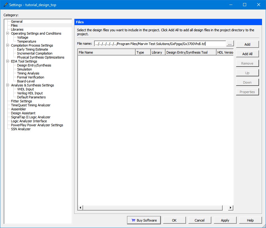
In order to configure the project as schematic entry and configure the pin assignment the TCL configuration script should be added to the project. To add the script to the project, click on Project | Add/Remove Files in Project… In the dialog box, click on the … button and browse for GX3700VHDL.tcl file in the “C:\Program Files\Marvin Test Solutions\GxFpga\” folder. On some systems, you may need to Click Open and then the Add button.

Add Tcl Script to Project
Then click on Tools | TCL Scripts … Select the configuration script file, GX3700VHDL.tcl and click on Run. This will configure your FPGA pin assignments.
Note: The TCL file will automatically add all the source files needed for the tutorial design to the Quartus II project.
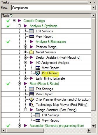
You can view the pin assignments by running the Pin Planner application which is found in the Tasks list as highlighted below:

Task Flow
The Pin Planner will display a matrix of the physical FPGA pins and their mapped names as well as the I/O standard supported by the pin. These mapped names are used in the FPGA design, as wire names and I/O pins, to connect to the physical connections of the FPGA.