This design will take two double word (32-bit) values, located in the first two double words in the Register space (byte offset 0x0 and 0x4), and add them together. The sum of the two values will be immediately output to the third double word in the Register space (byte offset 0x8). The sources for all referenced components are installed with the GXFPGA software package to C:\Program Files\Marvin Test Solutions\GxFpga\Examples\Quartus\Gx3700\ Tutorial_Verilog\source.
adder.v – An n-bit full adder.
and_gate.v - A two input and gate, the first input in n-bit width.
d_flipflop.v – A n-bit D flip-flop.
decoder.v – An n-bit decoder.
or_gate2.v - A two input or gate, the first input in n-bit width.
or_gate4.v - A four input or gate.
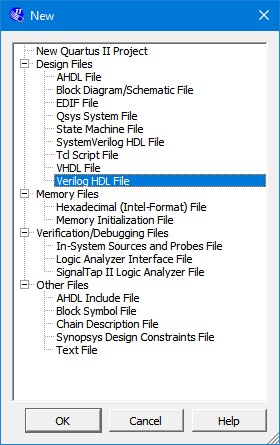
In order to open the Verilog text editor, click on File menu, and then New the following dialog appears.
Select Verilog HDL File:

New File Dialog Box
The top-level object for this project will be named tutorial_design_top.v. Start by creating module prototype with the proper inputs and outputs. The inputs and outputs all correspond to pin on the FPGA.
//--------------------------------------------------------------------
// Design Name : GXFPGA Verilog Tutorial
// Function : Demonstrates functionality described in the
// Verilog Tutorial chapter of the GXFPGA User's Guide.
//--------------------------------------------------------------------
module tutorial_design_top(Addr, WrEn, CS, PCIClock, PXI10Mhz, RdEn, FlexIO, LREAD_DV, FDt);
input [6:2] Addr;
input WrEn;
input [2:1] CS;
input PCIClock;
input PXI10Mhz;
input RdEn;
output [65:33] FlexIO;
output LREAD_DV; // Read Data Valid flag
inout [31:0] FDt;
endmodule
GXFPGA Verilog Tutorial Prototype
The first step is creating the circuitry required to decode the PCI Address when data is to be written from the PC to the FPGA. This circuit will be used in all three functions of this example project. The signals required for PCI Write access will be the PCI Clock, Write Enable, Chip Select 1, and some PCI Address lines. The PCI Address lines 5 to 2 will be fed to a decoder which will generate a 32-bit value, and the result will be ANDed with the Chip Select 1 bit. Each Chip Select bit represents a certain PCI BAR access (GX3700 has two bars, memory and register memories). Bit 1 represents BAR1 of the PCI memory space (bit 2 for BAR2). BAR1 is the general-purpose Control Register BAR for the GX3700. The results of the AND operation will be once again ANDed to the Write Enable PCI signal.
To create the address decoder, we’ll need to model the D Flip-flop (to latch the inputs), the And gate, and the decoder. For each module that we add, you should use the New File Dialog to add a Verilog HDL file to create the blank file. When saving, give the file the same name as the module. The source for the referenced modules follows:
//-------------------------------------------------------------------
// Design Name : and_gate
// Function : A two input and gate, the first input in n-bit width
//-------------------------------------------------------------------
module and_gate (out, in1, in2);
parameter width=1;
output [width-1:0] out;
input [width-1:0] in1;
input in2;
assign out = in2 ? in1 : 0;
endmodule
and_gate.v Source
When saving, give the file the same name as the entity. The source for the referenced entity follows:
//-----------------------------------------------------
// Design Name : d_flipflop
// Function : A n-bit D flip-flop
//-----------------------------------------------------
module d_flipflop (d, clk, ena, clrn, q);
parameter width = 1;
output [width-1:0] q;
input clk, ena, clrn;
input [width-1:0] d;
reg [width-1:0] q;
always @ ( posedge clk or negedge clrn )
begin
if (~clrn)
q <= 'b0;
else if (ena)
q <= d;
end
endmodule
d_flipflop.v Source
When saving, give the file the same name as the module. The source for the referenced modules follows:
//-----------------------------------------------------
// Design Name : decoder
// Function : An n-bit decoder
//-----------------------------------------------------
module decoder (decoder_in, enable, decoder_out);
parameter input_bit = 2;
output [2 ** input_bit-1:0] decoder_out ;
input [input_bit-1:0] decoder_in;
input enable;
assign decoder_out = enable ? (1 << decoder_in) : 'b0 ;
endmodule
decoder.v Source
In tutorial_design_top.v, we will now write the code to describe our PCI Address Decoder Circuit. Latch both the Address and Write Enable lines using the PCI Clock. Decode the 5-bit Address lines into a 32-bit bus named DecodedAddr. This decoded bus is ANDed with the FPGA’s CS[1] to define our PCI Address Decoded Select lines.
Additionally, we will define our Write Enable (WE) lines in this code block. We will use this later, along with Read Enable, to read and write to registers.
// PCI Address Decoder Circuit
wire [4:0] LatchedAddr;
wire LatchedWrEn, LatchedRdEn;
wire [31:0] DecodedAddr, WE, Sel;
d_flipflop inst23(WrEn, PCIClock, nc_ena, nc_rst, LatchedWrEn);
d_flipflop #(5) inst24(Addr, PCIClock, nc_ena, nc_rst, LatchedAddr);
decoder #(5) inst(LatchedAddr, nc_ena, DecodedAddr);
and_gate #(32) inst2(Sel, DecodedAddr, CS[1]);
and_gate #(32) inst3(WE, Sel, LatchedWrEn);
PCI Address Decoder Circuit
You will notice that we used a few undefined symbols in this last section: nc_ena and nc_rst. These are placeholders for enable and reset lines that our various components can take advantage of. For this tutorial, I have chosen not to use enable or reset lines at all so we should add the following code to tutorial_design_top.v to explicit set these wires to always enabled, never reset.
wire nc_rst, nc_ena;
assign nc_rst = 1'b1; // No reset
assign nc_ena = 1'b1; // Always enabled
Now that the PCI address decoder circuit is complete, we can feed the appropriate bits from the WE bus to D Flip Flops that will store data clocked in from the PCI data lines. For example, the first double word in PCI memory (representing the first number to be summed) will be written to a D Flip Flop with it enables line tied to WE[0] (the first bit in the WE bus). The second double word to be added will be written to another D Flip Flop with it enables line tied to WE[1]. Finally, the PCI Clock signal (33Mhz) will be used as the clock source of the D Flip Flops. Note that each bit of the Sel and WE buses represent a consecutive double word address (bit 0 corresponds with byte 0, bit 1 corresponds with byte 4, bit 2 corresponds with byte 8 etc.).
First we start by creating an extend circuit to deal with any timing issues with the WE signal. Then we will create some Flip Flops to latch inputs to the adders. We will use a placeholder named LatchedFDt as the input to the D Flip Flops. Eventually the PCI data lines will drive these inputs. Wire the outputs of the D Flip Flops to the Adder component. The output of the adder, Sum, will be used as an output later.
//-----------------------------------------------------
// Design Name : or_gate4
// Function : A four input or gate
//-----------------------------------------------------
module or_gate4 (out, in1, in2, in3, in4);
parameter width=1;
output [width-1:0] out;
input [width-1:0] in1, in2, in3, in4;
assign out=in1|in2|in3|in4;
endmodule
or_gate4.v Source
//-----------------------------------------------------
// Design Name : or_gate2
// Function : A two input or gate, the first input in n-bit width
//-----------------------------------------------------
module or_gate2 (out, in1, in2);
parameter width=1;
output [width-1:0] out;
input [width-1:0] in1, in2;
assign out=in1|in2;
endmodule
or_gate2.v Source
//-----------------------------------------------------
// Design Name : adder
// Function : An n-bit full adder
//-----------------------------------------------------
module adder (dataa, datab, result);
parameter width = 1;
output [width-1:0] result;
input [width-1:0] dataa, datab;
assign result = dataa+datab;
endmodule
adder.v Source
// WE[31..0] extend circuit - Extend write enable to mitigate timing issues
wire [31:0] LatchedWE, LatchedWE2, LatchedWE3, WE_EXT;
d_flipflop #(32) inst26(WE, PCIClock, nc_ena, nc_rst, LatchedWE);
d_flipflop #(32) inst27(LatchedWE, PCIClock, nc_ena, nc_rst, LatchedWE2);
d_flipflop #(32) inst28(LatchedWE2, PCIClock, nc_ena, nc_rst, LatchedWE3);
or_gate4 #(32) inst30(WE_EXT, WE, LatchedWE, LatchedWE2, LatchedWE3);
// Adder circuit - Latch the addends and include adder
wire [31:0] Sum, Addend1, Addend2;
d_flipflop #(32) inst4(LatchedFDt, PCIClock, WE_EXT[0], nc_rst, Addend1);
d_flipflop #(32) inst5(LatchedFDt, PCIClock, WE_EXT[1], nc_rst, Addend2);
adder #(32) inst7(Addend1, Addend2, Sum);
WE Extend Circuit and Adder Circuit
Before moving on we must first extend the RdEn signal. Add the following to the tutorial_design_top.v:
// RdEn to 2 PCI Circuit
wire RdEn_Extend;
wire [31:0] RE;
or_gate2 inst1(RdEn_Extend, RdEn, LatchedRdEn);
d_flipflop inst8(RdEn, PCIClock, nc_ena, nc_rst, LatchedRdEn);
and_gate #(32) inst12(RE, Sel, RdEn_Extend);
d_flipflop inst21(LatchedRdEn, PCIClock, nc_ena, nc_rst, LREAD_DV);
// RE[31..0] extend circuit - Extend read enable to mitigate timing issues
wire [31:0] LatchedRE, LatchedRE2, LatchedRE3, RE_EXT;
d_flipflop #(32) inst18(RE, PCIClock, nc_ena, nc_rst, LatchedRE);
d_flipflop #(32) inst19(LatchedRE, PCIClock, nc_ena, nc_rst, LatchedRE2);
d_flipflop #(32) inst20(LatchedRE2, PCIClock, nc_ena, nc_rst, LatchedRE3);
or_gate4 #(32) inst22(RE_EXT, RE, LatchedRE, LatchedRE2, LatchedRE3);
RdEn to 2 PCI Circuit and RE Extend Circuit
We also create a Read Data Valid output pin, LREAD_DV. This comes from a D-Flipflop with the PCIClock as an input clock and the RdEn as the input data. The D-Flip Flop also creates our extender for our ReadEnable.
The inputs to the D Flips Flops can now be wired to the PCI data lines (FDt). We need to clean up the FDt signal as is comes back into our circuit by adding the D-FlipFlop.
// Tri-stated FDt pins
wire [31:0] FDt, LatchedFDt;
reg [31:0] FDt_out_value;
reg [31:0] FDt_in_value;
assign FDt = RE_EXT ? FDt_out_value : 32'bz;
d_flipflop #(32) inst25(FDt_in_value, PCIClock, nc_ena, nc_rst, LatchedFDt);
reg [22:0] R; // Register for clock divider
assign IRQ = R[22]; //Assign MSB of clock divider register to IRQ,
//creates interrupts @ ~4Hz. ( 33 x 10^6 / 2^23 )
always @(posedge PCIClock) begin
if (RE_EXT[2]==1'b1)
FDt_out_value <= Sum;
else if (RE_EXT[0]==1'b1)
FDt_out_value <= Addend1;
else if (RE_EXT[1]==1'b1)
FDt_out_value <= Addend2;
else if (RE_EXT[31]==1'b1)
FDt_out_value <= result;
FDt_in_value <= FDt; //store the input value
R <= R + 1; //Increment clock divider register
end
FDt In/Out Signal Assignment
Now that the design has been completed, a revision number should be added so that the end user can read it back from the PCI bus at the 32nd register double word location (byte address 0x7C).
Including a revision number constant to the design is a Marvin Test Solutions standard practice that we recommend end users to follow. The revision constant is 32 bits long and is read as a hexadecimal number such as 0x3564A000. The first two digits of the hexadecimal number represent the company, in this case 35 is for Marvin Test Solutions designs. The next two digits are the design specific code, 64 in this case. And the last 4 digits, A000, is the revision of the design.
Add the following to tutorial_design_top.v:
// Add revision constant
reg [31:0] result = 32'h3564A000;
Symbol Properties