
The GX3700 consists of a user programmable FPGA that can access external resources and peripherals such as the PCI bus, SRAM and flash memories. The user FPGA is an Altera Stratix III that can be programmed directly through the software driver or indirectly by the onboard EEPROM that can store a FPGA bit stream for later use. An Expansion board connects to the User FPGA to provide external I/O. The standard expansion board provides 160 I/O channels that are brought out to the front panel. The user may design custom expansion boards based on documentation provided by Marvin Test Solutions.
.
GX3700 Architecture
The Gx3700 has three types of memories, internal SRAM, external SRAM and Flash memory.
Inter-FPGA Bus Interface Diagram figure is a more detailed block diagram of the connections between the User’s FPGA, the Flash and the SRAM:

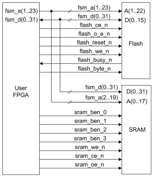
GX3700/GX3700/e Connections between User FPGA, Flash, and SRAM
The User FPGA, Stratix III, can be configured either through the EEPROM or directly through the PXI Interface. It has access to PXI resources such as the local bus, trigger bus, and PXI 10MHz clock source and is also connected to the PXI Interface FPGA to give access to PCI resources and memory. This allows the User FPGA to communicate with the host system’s operating system using the provided GXFPGA software library functions.
A more detailed diagram of the PXI/PXIe Signal Connections is shown below . It shows the different PXI/PXIe signals and how they are interfaced to the User FPGA.
The bi-directional bus switch with level shifting allows the PXI/PXIe signals to be interfaced to the User FPGA. The direction of the signals is controlled and determined by the signals from the User FPGA.
For example, to use the signal PXITrig(7), the user FPGA would be programmed as follows:
1. If this signal is only used as an input, define it inside the User FPGA as an input pin.
2. However if the signal is used as an output only or a bidirectional I/O, define it as such in the User FPGA but make sure to drive the output to high impedance or tri-state level when the signal is not driving or is inactive.
In both of these cases the level translation and the direction of the signals are handled by the on board bus switch.
Also shown are the buffers for the DSTAR_A, DSTAR_B and DSATR_C signals. These buffers conform to the standard as required by the PXI Systems Alliance’s PXI Express Hardware Specification Rev 1.0.
Note that the DSTAR signals are only available with the GX3700e module.

PXI/PXIe Signal Connections