I/O Channel Block Diagram
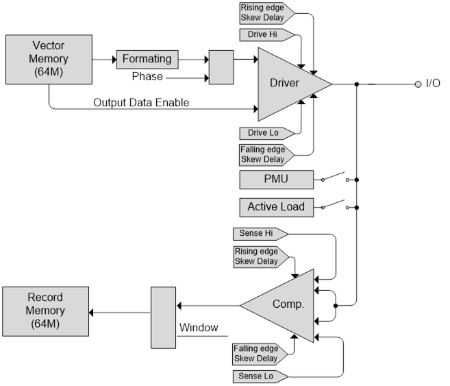
The figure above is a block diagram of a single I/O pin. Up to 16 boards can be used in one domain for a maximum of 512 pins (each board containing 32 I/O pins). Output data, which is stored in the Vector memory, is outputted from the board as a function of the PHASE signal through the Driver when enabled; the encoded data (see Memory Management) enables the Driver output when the specified Vector is defined as an output Vector. The output data to the UUT will also be stored in the Record memory via the receiver pin electronics. The output data will be formatted as it was defined programmatically by the user to one of the following formats: No Return, Return to Zero, Return to One, Return to Hi-Z, Return to Complement, Surround Complement.
Each data channel’s output signal has programmable Drive Out Hi and Drive Out Lo levels. The Drive Out Hi level can be set from -2 volts to +7 volts and must be greater than the output driver’s Drive Out Low voltage. The Drive Out Low voltage can be set from -2 volts to +7 volts.
The pin electronics input analog stage is comprised of a set of constant current sink and source loads, and clamping (commutation) sink and source voltages. In addition, the input channel’s programmable load can be set to have constant source and sink current loads up to +24 mA and -20 mA with 0.3662 μA of resolution. The input channel’s current source will force the specified constant current to be active when the input voltage is above the high (or low) voltage clamp or commutation value. Each input channel’s constant current voltage clamp can be set programmatically. With independent high and low clamping (commutation) voltages, the source and sink current each have their own commutation voltage level. In addition, each channel can be programmed to a termination voltage value (VTT). Note that VTT and VComm share a common voltage source, which allows only one mode to be supported for each channel.
The input signal is connected to two comparators. The threshold sense high and low voltage levels are set programmatically by the user. Both the input high and low voltage threshold values can be set from -2.0V to +7.0V. Each channel’s operating temperature, drive high / drive low voltages, and sense hi / sense lo voltages can all be monitored and measured.
Input data is stored in the Record Memory for the response record mode and is stored at the rate of the Vector Clock. The Vector opcode, once decoded, (see Memory Management) enables the input when the specified step is defined as an input step.
The input data will be processed as follows:
● If input data is higher than the high voltage threshold, the input is detected as logic high. Data will be logged as logic high to the record memory.
● If input data is lower than the low voltage threshold, the input is detected as a logic low. Data will be logged as a logic low to the record memory.
● If input data is higher than a low voltage threshold and lower than a high voltage threshold, input is invalid. Data will be logged as a logic low to the input memory and logged as a 1 to the invalid data memory.
Note: Each channel’s output and input are connected. As a result, whenever a channel is defined as an output for a specified step, the corresponding input channel can monitor / record the channel’s output providing drive / verify functionality.
Each channel has a constant current source and sink load currents and a corresponding voltage clamp that can be set and enabled programmatically. This programmable feature allows the user to test an external UUT under load. When constant current source and sink load currents are enabled, the specified channel’s driver state is set to Hi-Z
The input channel’s current load will provide a constant current source when the input voltage is above the specified commutating voltage, and will provide a constant current sink when the input voltage is below the specified commutating voltage. The constant current source and sink values can be set from -20mA to +24mA with 0.3662 μA of resolution.

GX5296 Input Load Current Voltage Clamps
Each channel has a high-speed dual voltage comparator with its own independent threshold setting. Each channel’s high and low input voltage threshold comparators can be set programmatically. There are two threshold voltage level settings for each input channel: logic high level and logic low level. Each input channel can detect three voltage levels: High, low and undefined. When the input voltage is equal or greater than the threshold logic high, a logic high is recorded. When the input voltage is equal or less than the threshold logic low, a logic low is recorded. When the input voltage is between the threshold high level and the threshold low setting then the value is recorded as an in-valid logic level.
The input high and input low voltage thresholds can operate over a range from --2.0V to +7V with the high threshold higher than the input low voltage threshold and the low voltage threshold lower than the input high voltage threshold.
The Input channel’s low and high threshold voltages can be read back and set dynamically at any time even when the DIO is in the run state.
Each output channel’s data can be formatted as follows:
No Return |
The output logic level stays either high or low for the duration of the clock period (default). |
Return to Zero |
The signal returns to zero during the phase return edge within a clock cycle. |
Return to One |
The signal returns to one during the phase return edge within a clock cycle. |
Return to Hi-Z |
The signal returns to Hi-Z during the phase return edge within a clock cycle. |
Return to Complement |
The Return to Complement (also called Manchester code) format ensures that each transmitted data bit has at least one transition during the phase return edge within a clock cycle. It is, therefore, self-clocking, which means that a clock signal can be recovered from the encoded data. Return to Complement ensures frequent data transitions which are directly proportional to the clock rate which helps clock recovery. A logic low is expressed by a low-to-high transition. A logic high is expressed by high-to-low transition. The transitions which signify logic high or low occur at the midpoint of a period, the direction of the mid-bit transition indicates the data. |
Compliment Surround |
Tristate driver from beginning of vector to assert time and then drive programmed level. Tristate driver at return time. |
Force Zero |
Force driver to low level. |
Force One |
Force driver to high level. |
Force Off |
Force driver to Hi-Z. |
Force Inverted Phase |
Drive high to low at the phase assert edge and low to high at the phase return edge. |
Force Phase |
Drive low to high at the phase assert edge and high to low at the phase return time. |
NOTE: the specified channel data format will be applied to all the channels’ vectors that are set as outputs. The inputs do not support or decode formatted data.
Each digital channel includes a parametric measurement unit (PMU) which can be used to characterize and measure a digital pin’s DC characteristics. The PMU can be configured for force current, measure voltage, or force voltage, measure current. The PMUs associated with the 32 digital I/O channels offer the following capabilities:
Force voltage: -1.5 volts to +7 volts.
Measure voltage: -1.5 volts to +7.
Force current: +/- 32 mA FS, +/- 8 mA FS, +/- 2 mA FS, +/- 512 uA FS, +/- 128 uA FS, +/- 32 uA FS, +/- 8 uA FS or +/- 2uA FS.
Measure current: +/- 32 mA FS, +/- 8 mA FS, +/- 2 mA FS, +/- 512 uA FS, +/- 128 uA FS, +/- 32 uA FS, +/- 8 uA FS or +/- 2uA FS.
Measurement resolution is 16 bits for both voltage and current measurement functions. Note that while each channel has a dedicated PMU, the measurement resource is shared between all 32 channels, requiring sequential measurement of each channel.
The figures below detail the PMU’s four quadrant V-I capabilities. Note that for the 32 mA and 8 mA current ranges, a commutation voltage of +1.75V or higher must be maintained to achieve accurate source / measure currents from -6 mA to -32 mA. This is due to the limited headroom associated with the pin electronics when operating in PMU mode.

PMU Measure Current V-I Operating Range

PMU Source Current V-I Operating Range