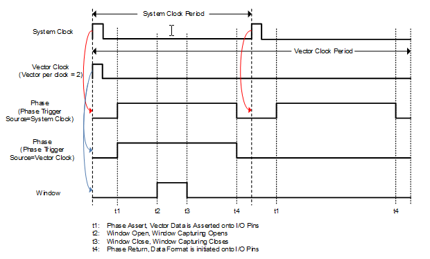
The GX5296 Timing Subsystem is comprised of the System Clock, the Vector Clock and a Timing Generator which generates the Phase Assert, Phase Return, Window Open, and Window Close signals. The System Clock Cycle in conjunction with the clocks per vector value determines the base frequency at which Vectors assigned to the current Step, will be clocked from the Vector Memory. The Vector Clock period is equal to the System Clock period multiplied by the Clocks per Vector value (1 to 256). The Phase and Window signals determine how and when (in conjunction with the Data Format) a Vector’s output state will be applied to the I/O Pins within a System /Vector Clock cycle. The Phase Trigger Source setting determines which clock (System or Vector) will cause the Phase signal to reset and begin again.
A timing set group consists of up to 8 a Phase Assert/ Phase Return and 4 Window Open / Window Close strobes. The timing sets are used to control the DIO channel drivers and receivers.
A Phase controls the driver output operation and consists of an Assert and a Return edge. The Assert signal loads the current pattern code in to the output driver. The Return signal is used to enable the format code in the driver. The Return signal is not used for the Non-Return format code.
The Window controls the signal capture for the receiver and consists of an Open and Close edge. Each channel can be set to one of two capture modes. In Open Edge mode, the Window Open edge strobes the channel comparator input and the Close Edge is ignored. In Close Edge mode, the Window Close edge strobes the channel comparator input and the Open Edge is ignored.
The Phase timing logic can be triggered by either the System Clock or the Vector Clock. The Window timing logic is triggered by the Vector Clock.
A timing diagram of the System Clock, Vector Clock, Window, and Phase signals is shown in the figure below:
System Clock, Vector Clock, Phase and Window Timing Diagram
Timing Set groups are used in conjunction with the Indexed Timing Set mode, with each sequencer step pointing to any of the 64 timing set groups located in the Timing Set Index Memory. Each timing set group is composed of up to eight pairs of Phases and 4 pairs of Window settings. Phase and Window timing is assigned to each channel, based on the application’s specific timing requirements. A common application might be the emulation of a CPU bus with read and write cycles. Assigning specific phase and window timing values for the read and write cycles greatly simplifies the emulation of bus cycles. By mapping the “write” phase and window to one time set index value and the “read” phase and window to another time set index value, the emulation of bus cycle timing is simplified.
The user can assign the 8 phases and 4 windows to any I/O channel or a range I/O channels. Once assigned, the user can create up to 64 timing set groups which can be accessed via the timing set index for each sequence step. Each step can be assigned to one of the 64 Timing Set Index numbers, while the channels will maintain the assigned Phase and Window TSet settings.
The figure below details the relationship between the time set index, time set groups, and I/O channel assignment.

Indexed Timing Sets Diagram