The GX1120 contains a PXI interface device as well as an FPGA which is configured to support DDS or AWG operation which essentially provides all of the digital logic for waveform generation. Configuration of the FPGA is performed at power up or via a driver function call prior to programming the module’s waveform generation parameters.
Analog components include a 12-bit A to D converter that supports external modulation functionality as well as a programmable offset generator, a programmable output amplifier, and multi-pole low pass filters. The output stage is common for both DDS and AWG operation modes with two different filters to optimize noise and spectral performance, based on the specific mode of operation.
The AWG includes sequence and waveform memory configured as 32M by 16 bits. A PLL based clock generator for each channel provides a programmable sample clock rate from 10 mHz to 250 MHz with a resolution of 4 digits or .01 Hz - whichever is lower. The reference for the PLL is an internal 50 MHz oscillator, the PXI 10 MHz clock, or an external 10 MHz input via the front panel connector. The minimum waveform sequence length is 2 points. Waveform sequencing includes the ability to loop continuously, loop once, sequence between defined start and stop addresses or loop (burst) N times.
The DDS mode utilizes 8K by 16 bits of waveform memory. Standard waveforms are loaded into the waveform memory when the FPGA is configured, eliminating memory load times at run-time. Standard waveforms include sine, triangle, ramp (up or down), pulse, square and noise.
Each channel can accept an input trigger from the PXI trigger bus, an external front panel input, or a software trigger. Separate marker and synch outputs for each channel are available on the DB-15 front panel connector and the SMB connectors respectively.
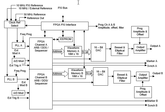
A block diagram of the GX1120 is shown in the figure below. Each channel’s FPGA can be configured to operate in Arb or DDS mode.
GX1120 Block Diagram

GX1120 Board Side View