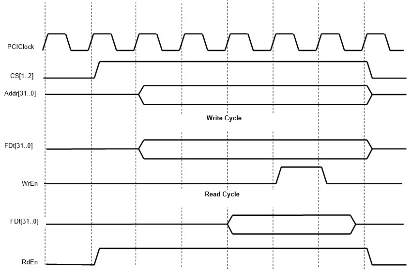
The following graph describes the PCI Signal timing information in relation to the user FPGA (Cyclone III). You can use this information to help in the design of the PCI address decode, read and write circuitry within the user FPGA configuration. Refer to Table Pin Assignments Table for information on the pin alias description. The use of these pins is shown in the GXFPGA Tutorial and Example (Phase 1, 2 and 3), where they are used to communicate with the PCI bus and host computer.
Note that the PCIClock signal’s period is assumed to be equal to the period of the 33 MHz PCI Clock (30.3 nS).

Legend:
PCIClock – PCI Clock, 33 MHz.
CS[1..2] – Chip Select 1 or Chip Select 2.
WrEn – Write Enable. When high, rising edge of the clock writes data.
RdEn – Read Enable. When high, User FPGA can drive the data bus.
Addr[2..19] – Address bus. Address lines 17..2.
FDt[31..0] – Data bus. Data lines 31..0. In a read cycle data must be valid during indicated period.