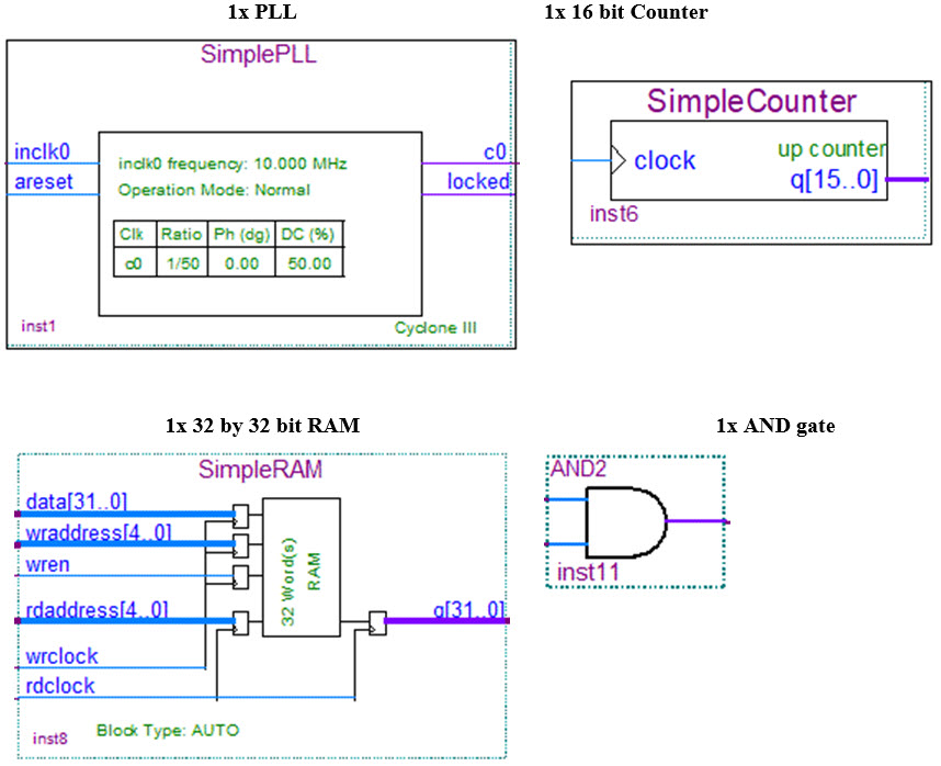

Phase 3 - Dynamic Digital Sequencer Components
This design functions as a simple dynamic digital pattern generator. A PLL drives a Counter which iterates through a 32 double word memory that outputs 32-bit wide digital patterns to the I/O Pins. The memory is loaded through the PCI bus, allowing users to program the device with vectors through the software front panel or the DLL API.
This phase will require the use of the MegaFunction Wizard to generate all three components, PLL, RAM, and counter. The wizard will allow you to customize the component for this particular application. The generated component will be stored in a file (.qip) that will automatically be included in the project.
First insert the PLL component by double clicking on an empty space in the design and clicking on MegaFunction Plug-In Manager. Choose to create a new MegaFunction variation and click Next. Then select the symbol called ALTPLL under the I/O folder. Name the new variation SimplePLL and click Next. The next dialog box will prompt you for the input clock frequency. We will be using a 10Mhz reference clock source so enter 10Mhz into this field.
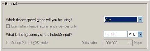
PLL Wizard Dialog Box 1
Proceed through the next few screens, with the default choices until you get to step 3 in the wizard entitled Output Clocks. Select 50 as the division factor as shown in the following figure:
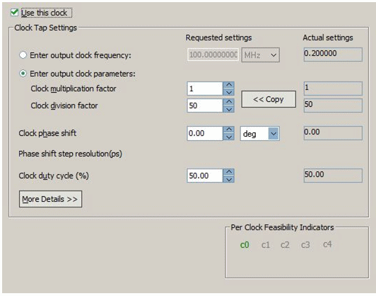
PLL Wizard Dialog Box 2
Click Next for the rest of the windows until you get to the last window showing you the files that will be created and then click Finish. The customized component will now be included in your project automatically so that you can start using it. Click OK to return to the design view, and then place the newly created symbol on your design.
Attach a wire to the inclk0 terminal of the PLL symbol, and name the wire 10Mhz. This will connect the wire to the 10Mhz input pin that has already been created in the phase 2 design.
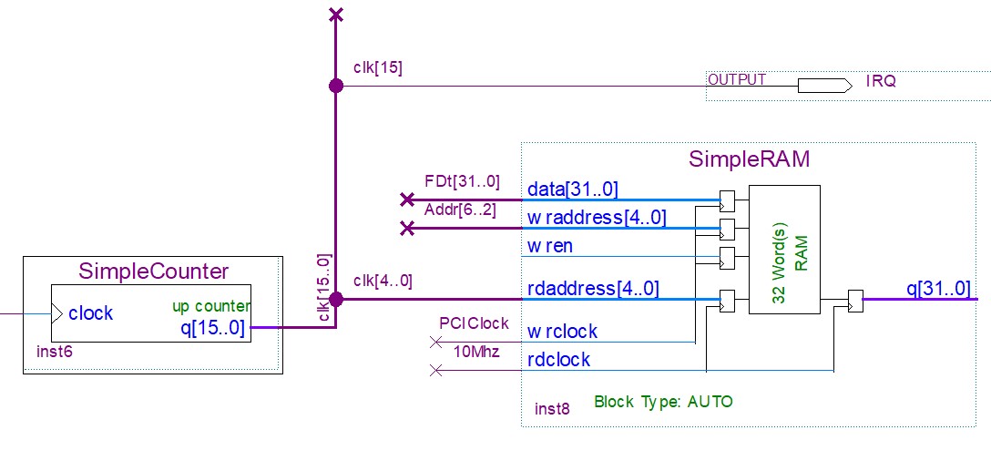
Repeat the previous steps to create a new custom component using the MegaFunction Wizard and select LPM_COUNTER from the arithmetic folder. Name the custom component SimpleCounter and click next. Select 16 bits for the output bus width. You can now click next for the rest of the windows and finally click finish to place the symbol on your design. Wire the c0 output terminal from the PLL to the clock input on the counter and connect a bus named clk[15..0] to the output of the counter as shown in the figure below.
The last component needed is a 32 double word RAM. You will need to deploy the MegaFunction Wizard once again, and select the 2 port RAM component from the Memory Compiler folder. Call the new component file SimpleRAM and click Next. Make sure to select 32 as the word length and 32 as the input width as the following figure shows:
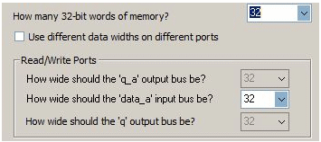
RAM Wizard Dialog Box 1
In the next window make sure to select a dual clock for reading and writing so that data can be written to the RAM from the PCI bus and read out to the IO pins concurrently.
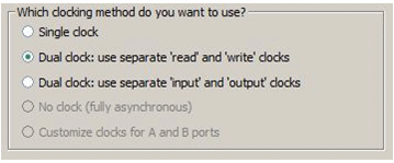
RAM Wizard Dialog Box 2
Click Next on the rest of the windows and click Finish placing the RAM component on your design. Now connect the least significant 5 bits from clk[15..0] (clk[4..0] coming out from the counter) to the read address, rdaddress[4..0], of the RAM component. Then wire the MSB (clk[15]) of the counter output bus to an output called IRQ to generate interrupts, as shown in figure Counter, IRQ_and RAM_Circuit.
Connect a bus to data[31..0] and wraddress[4..0]. Name these busses FDt[31..0] and Addr[6..2] respectively. Then connect wires to wrclock and rdclock and name the wires PCIClock, and 10Mhz respectively.
You will need to place an AND gate next to the RAM component and wire a new input pin called CS[2] and a wire named WrEn to it. The output of the AND gate should be connected to the wren input of the RAM. This AND logic ensures that only BAR2 PCI accesses are able to write to the RAM. This will allow us to use the FGPA Memory space to write out digital patterns to the sequencer instead of the FPGA Register space (which is being used for control). Note that when CS[2] is high, it signifies an access from BAR2.
Finally create a bus connected to the q[31..0] output from the RAM and name it FlexIO[64..33]. This connects the RAM output to the 32 physical IO pins.
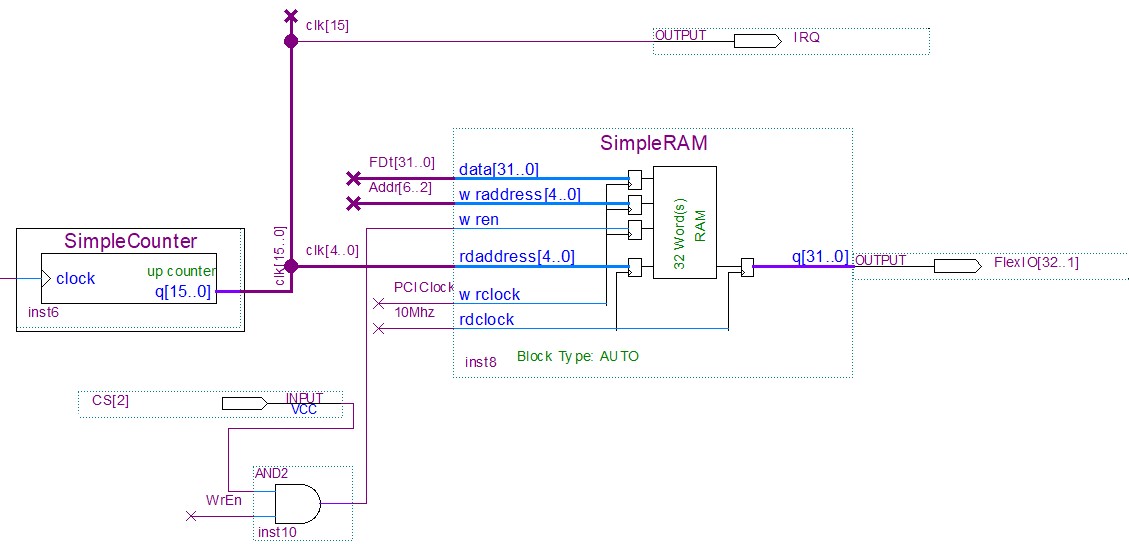
Dynamic Digital Sequencer and IRQ generating Circuit
At this point the design is complete, continue with the next sections to generate SVF or RPD files and load your design to the GX3700.