Welcome to our first issue of Test Connections for 2017. If you are a first time recipient, welcome! And, if you have been following us through our newsletters for a while, welcome back!
Q-1 is proving to be both challenging and successful, as we expand our offerings for our military, aerospace and manufacturing customers. In fact, in all areas there are some exciting developments, including enhancements we are offering to legacy semiconductor test sets.
Many of you have expressed great interest in our advanced test solutions that make test easyTM from the factory to the flightline and to the depot for military and aerospace customers. The same excitement is being exhibited in the production arena for our manufacturing customers.
Our suite of solutions supporting armament test - including the MTS-3060 SmartCan™ Universal O-Level Armament Test Set - has been featured and a big attraction at many recent trade shows and events. If you were not able to attend, we invite you to explore our web site or contact us to learn more.
With a great 2016 behind us, we look forward to working with you in 2017, delivering innovative test solutions and offering unrivaled long-term support.
We hope you enjoy this month's issue of Test Connections which includes new product updates and news events.
Please send your comments or suggestions regarding this newsletter to marketing@MarvinTest.com.

TS-217A Universal Armament Test Set |
Marvin Test Solutions has recently upgraded the TS-217, a Universal Armament Test Set which supports a variety of launchers, pylons, and bomb racks as well as suspension and release equipment, providing full parametric test and troubleshooting capabilities. | 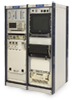 |  Read more Read more

Trade In Your Legacy Test System! |
Trade in your legacy Teradyne L2xx or L3xx, GenRad 275x, Schlumberger S790, or VXI-based system and get a discount of up to $500,000 on a new GENASYS single-bay or two-bay system with enhanced capability and PXI flexibility. |  |
Read more

User Programmable FPGAs |
Field Programmable Gate Arrays (FPGAs) are an integral part of today’s electronic products. Marvin Test Solutions’ FPGA products offer users the flexibility to create high-performance, customized PXI instrumentation for both digital and mixed-signal applications. | 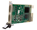
|
Read more
|

ATEasy® 10 Beta 3 is Available for Download:Read on
to learn more.

How to Modify ATEasy HTML Test Log Tests Table Click here
to learn more.

Would you like to receive the Test Connections Newsletters on a regular basis?
You can
sign up
at any time.
Can't find what you're looking for? We'll build it for you. We also customize and
adapt standard catalog products to meet your specific needs. Click here to request more information.
|